|
The csp's small size presents new
challenges in the rework process. although rework of csps is
similar to rework for bgas, the tolerances for solder paste and
flux deposition are greater.
Chip-scale packages, because of
their diminutive size, present new challenges in the rework
process compared to conventional package formats. The most common
CSP today is Tessera's µBGA?package at 30 mil, 0.75 pitch,
which is now in production by Intel and others with 40-56 solder
balls.
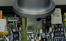
Figure 1. Removal of a CSP in an encapsulated
enviroment virtually eliminates adjacent compnent heating, since
exhaust ports are located toward the top of the rework nozzle.
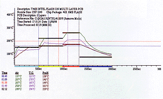
Figure 2. This four-stage rework profile,
duplicates the original manufacturing profile.
Most PCMCIA cards and cellular
phone boards employing CSPs are hard to hold. The edges are packed
with connectors and sockets, and a special holder has to keep the
PC board level and firm during rework.
These small PC boards are often 20 mil thick and are double-sided,
making them quite susceptible to damage by heat. The boards often
contain perimeter CSPs with ball counts as high as 196 on 20-mil
pitch.
The reflow of adjacent parts is the most difficult to address
because some manufacturers place discretes within 20 mils of the
CSP.
Rework suppliers will feel more comfortable with 50 mil as a
standard "keep out" zone. If customers insist on placing
parts closer than 50 mil, then they should expect to pay for a
custom tool to rework and remove the part.
Future
CSP Challenges
Higher
I/O (up to 625) will be common and 20 mil will be the normal pitch
in the future. Finer pitches down to 12 mils are now being
discussed by many device manufacturers, with 8-mil and 4-mil ball
size. Some high power parts may also use solid copper balls
instead of eutectic solder balls. This will require an increase in
the stenciling of solder paste during CSP rework.
Benefits
of CSP parts
CSP
packages are light and robust compared to a TSOP or QFP. As a
result, the components will self-center easily. BGA parts also
self-center, but contain a much larger solder ball, which requires
more heating due to its size.
The term "BGA" is becoming more commonly associated with
larger area array packages, while "CSP" refers to any
package whose area does not exceed 1.2x that of the die.
CSP
Rework Process Overview
Rework
of area array CSPs is quite similar to that practiced with BGA-packaged
devices except for tighter tolerances, especially in the solder
paste or flux-deposition process.
Although CSPs have superior self-centering characteristics, one
must consider that greater alignment accuracy is required due to
their smaller scale. The µBGA CSP features a ball size of
.012", so placement should be within 50% =.006" or less.
If via construction is employed for this package, then the
accuracy should be much tighter, otherwise solder paste might be
pushed into the via during placement or reflow. Safe component
removal begins the rework process. Degradation to the PC board,
CSP and solder connections can be avoided by closely adhering to
rise and dwell times prescribed by the solder paste and component
manufacturers. To ensure time-and-temperature accuracy,
microprocessor-controlled heating, including a preheat, thermal
soak, reflow and cool-down zone should be employed. A controlled
dwell time in each zone should be permitted.
The ideal thermal profile is typically a duplication of the
original production reflow profile, although refinements can be
made in the rework environment, when justified. For example, it
may be that the original reflow profile was not optimized for the
component being reworked, therefore, modifications are needed to
compensate.
The removal process can be slightly different from the replacement
profile, but generally the preheat and soak are the same. This is
usually a function of mass due to the PC board and the number of
board layers.
The reflow zone is usually between 20 and 60 seconds, but this
depends on the type of solder paste and other factors. The reflow
zone is the only zone that should be shortened for CSPs. To remove
the part, we do not need to be in reflow for 60 seconds, as long
as we can guarantee that reflow is complete so that removal can
safely take place.
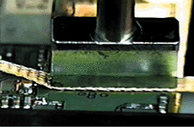
Figure
3. Residual solder removal with desoldering braid and
low-temperature, highly thermally-stable conductive tool.
Reflow
Profile
A
four-stage rework profile duplicates the original manufacturing
profile.
Other
methods of controlling the quality of the rework process include:
1.
Thermal energy should be directed through the component
body to the solder joints without heating adjacent components.
2.
Heating should ideally take place in an encapsulated, inert
gas-purged environment (Figure 1), where temperature gradients do
not exceed ?罜 across the heating zone. This condition will
facilitate simultaneous reflow of all solder joints. It will also
avoid inadvertent pulling of pads during component removal. Lack
of oxidation on thermocouple or RTD will ensure accurate
temperature readings (another advantage of inert processing, which
can sometimes be neglected).
3.
During the reflow profile, the utilization of a convective bottom
side preheater will maximize temperature uniformity, reducing top
and bottom PC board temperature gradients across the area to be
heated.
4.
Automated component lift-off can further enhance process control.
Virtually all CSP rework systems use hot gas or hot air as their
thermal transfer medium. Interchangeable nozzles designed with
different geometries are used to accommodate different
applications and to direct the airflow path.
When choosing the appropriate nozzle for CSP
rework, keep in mind that it should be as large as possible so
that the operator does not inadvertently "bump" the
component, but not so large that it will contact adjacent
components. Exhaust vents located near the top of the nozzle will
prevent heating of adjacent components.
Temperature
Measurement
During the initial
stage of profile development, accurate temperature measurement can
be obtained directly at the solder joint. Theoretically,
thermocoupling of solder joints is critical, but the lack of space
between the CSP and PC board makes thermocoupling difficult.
If the component is soldered with solderpaste in production with a
standoff height of .010 mil or greater, a small thermocouple can
be inserted between the part and the PC board with success.
Another possible method of thermocoupling is to drill a small
diameter hole (slightly larger than the diameter of the
thermocouple) through the bottom of the board to touch the
ball/pad interface directly. This can only be done if a PC board
can be spared. This method will allow the realtime solder-joint
temperature to be fed back to the microprocessor controller. The
operator will then be able to make "on-the-fly" changes
to the time/temperature parameters based on this feedback while
the profile is active.
Since the recommended rework system provides low temperature
gradients (< 5°C) across the heating area, the temperature
measured at that one particular solder joint/pad interface will be
within a few degrees of the entire array of solder joints,
ensuring profile repeatability and accuracy.
Although it is not practical to drill into the board, the profile
parameters recorded during initial profile establishment (removal)
can be utilized for subsequent attachment profiles. Air velocity
should be kept at a minimum of about 15 l/m as a starting point.
Excessive airflow settings can inadvertently cause the CSP to skew
during reflow, especially in the cooling zone when solder is
solidifying.
Vacuum lift-off should be automatically engaged at the transition
point between the reflow and cool-down cycles without applying any
stress to the solder joint. A low specification of vacuum (i.e.,
<15" Hg) will protect the pads from damage by allowing the
vacuum seal to break if all the joints have not exceeded reflow
temperatures, yet will provide enough vacuum to lift any CSP
despite its total mass.
Land Preparation
Once a CSP has been
removed, the site must be cleaned to prepare for package
attachment. Care is critical; coarse or improper procedures can
burn, lift-off or otherwise damage the delicate attachment area.
The best results will be achieved with a low-temperature,
blade-style conductive tool (matched specifically to the width of
the pad array), in conjunction with desoldering braid (Figure 2).
The ideal conductive tool will provide maximum heat transfer at
the lowest possible source temperature, thereby maintaining
temperature stability. Rapid heat transfer will protect the
integrity of the PC board. High temperatures are definitely not
recommended.
The flux content of the desoldering braid must be compatible with
the flux residues contained in the removed solder paste and with
the paste or flux that will be used for placement. Active fluxes
can be used effectively only if the area is properly cleaned and
inspected before placement.
Due to the difficulties associated with cleaning in the tiny space
between the CSP and PC board, the use of "no-cleans"
throughout the entire process is recommended.
The process of employing a bottom-side convection preheater is
also recommended during the residual solder removal process. This
step will decrease top and bottom temperature gradients, further
eliminating any accidental pulling of fragile pads.
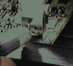
Figure 4. When the
stencil is aligned, printing can be done.
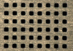
Figure 5. Example
of artwork stencil apertures.
Eutectic Solder
The
above process assumes that the solder bumps are composed of
eutectic (Sn63/Pb37) solder, although some CSPs employ high
temperature (Sn10/Pb90) solder spheres that are attached to the
board with lower temperature (Sn63/Pb37) solder fillets. If the
removed CSP contains these high-temperature spheres, not all of
them will remain on the package after removal. Some
high-temperature spheres will adhere to the package while others
will remain on the board.
Melting the spheres is not recommended, since this practice will
alter the metallic composition of the pad, resulting in an
alteration of the reflow point during the subsequent attachment
stage. To remove high-temperature spheres, heat the land area past
eutectic temperature and "pluck" the high-temperature
spheres from the PC board with tweezers.
This removal can be accomplished by "hovering" the
rework nozzle above the land area (while maintaining the
bottom-side heating). During the high-temperature solder removal
process, the eutectic solder should be kept above reflow
temperature.
After all the high-temperature spheres are removed completely from
the PC board, residual eutectic solder can be removed with
desoldering braid and a thermally-stable conductive tool at a low
temperature.
Once all residual solder has been removed from the lands, they
should be cleaned with an approved solvent, preferably one
prescribed by the solder manufacturer. At this point, the operator
can inspect for any neglected solder splashes or degradation to
the printed circuit board.
Accurate
Solder Paste or Flux Deposition
Most CSPs contain
bump matrices in the area of 0.5mm to 0.8mm pitch, which create a
significant challenge for depositing solder paste in the rework
environment (Figure 4).
The ideal method for
depositing solder paste in a precise, uniform fashion is through
the use of an individual component miniature stencil, similar to
the practice in the assembly environment.
Since alignment of the stencil apertures with the mating PC board
lands can be difficult by eye (the pads are only 12 mil in size),
this can best be done under 50x - 100x magnification using the
prism to align.
Once precise alignment is accomplished (Figure 3), the stencil can
be lowered onto the PC board, where the paste is applied with a
small, metal squeegee blade. The width of the squeegee blade
should be matched to the stencil, enabling the user to make one
single pass to avoid any overprinting.
Since this is a manual printing process, technological advantages
should be designed into the rework stencil. The optimum rework
stencil should be trapezoidal laser-etched (tapered), so that the
opening on the bottom of the stencil is 1-2 mil greater than the
top opening. Square apertures are preferred, as opposed to
circular apertures, with a radius on all four corners of each
aperture (Figure 5).
Transfer
Characteristics
Conforming to the above stencil specifications will significantly
enhance solder paste transfer characteristics. Although excellent
results have been recorded utilizing a standard -325 /+500 mesh
size solder paste, a high-viscosity (i.e. >900 kcps) paste is
strongly recommended. A no-clean flux should be specified, since
cleaning beneath the CSP is virtually impossible.
Not every CSP manufacturer endorses the application of solder
paste during the rework or assembly process. Certain manufacturers
recommend only the application of a gel-based, high viscosity
flux. Higher viscosity is recommended to provide adherence between
the CSP and PC board during the rework/assembly process. For best
results, use solder paste only if the stand-off height and
strength are the same as the production PC board. The cost of the
board and the reliability required also affects which process刾aste
or flux刬s preferred.
Component
Placement
CSP placement is notably similar to that of a BGA package. Both
types contain I/Os in a bottom-sided array matrix, therefore,
precise alignment between the solder bumps and mating land pattern
cannot be achieved by eye. Alignment should be made through the
utilization of a split-beam optical system where a dual image of
the CSP solder bumps and mating land pattern can be viewed and
overlaid on a high-resolution monitor (Figure 6).
Due to the small specifications associated with CSPs, alignment
should be achieved within the window of 50x - 100x magnification.
The optimum placement machine should give the operator the ability
to make fine adjustments between the overlaid images in the X, Y
and rotational axes. A CSP can properly align itself during reflow
even if it is as much as 50% misaligned with the mating pads. Keep
in mind, however, that the CSP's tiny specifications make 50% a
fine tolerance.
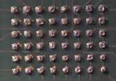
Figure 6. An
Optimum rework stencil
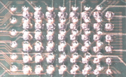
Figure 7. Dual
image of alignment of CSP solder bumps and solder paste pattern
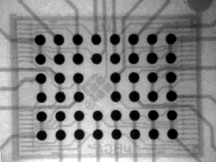
Figure 8. X-ray
inspection of passed CSP; All solder joints are uniform in
appearence with no evidence or voids or bridging.
Reattachment
Since the optimum
rework profile parameters are developed during the initial removal
process, the same reflow profile can be used for reattachment as
well as for subsequent removal processes.
No additional thermocouple feedback or operator dependency is
required, since all parameters are optimized during the removal
profile and stored in the memory of the rework system. Therefore,
profiles can be recalled with the touch of a button for both
placement and removal.
One must not take shortcuts by shrinking the duration of the
reflow profile simply because the CSP is a tiny component.
Unlike traditional leaded SMDs, the human eye cannot verify solder
joint integrity, since the array of interconnections is hidden
beneath the CSP. As with BGA inspection, X-ray equipment is the
only optical method of inspection available today (Figure 7).
Although one can electronically test the final assembly for
functionality, this method does not allow for verification of
solder voids or optical measurement of solder volumes (i.e.
inconsistent or excessive solder paste deposition).
The high reliability of well-controlled CSP rework processes
actually makes the latter a reasonable alternative.
As with BGA packages, simple "touch-up" of discovered
defects is not possible. Correction of any defect calls for the
removal of the entire component, followed by the entire rework
cycle. The impact, however, can be minimized by strict control of
the rework process.
CSP Cleaning凥ow
Feasible?
Removing contaminants
or even inspecting for residue in the minute spacing between the
CSP and PC board is generally impossible. Consistent use of
no-clean fluxes on CSP assemblies is recommended for eliminating
the need for cleaning. Remember, if a gel flux is used to rework
the part, then the stand-off height of the component is virtually
non-existent. When solder paste is used, a stand-off height is
present so some cleaning can be done if needed.
Conclusion
Chip-scale packages
share many positive attributes, as well as challenges, in the
rework process with their larger predecessor, the ball grid array.
By far the most challenging aspect of the CSP rework process is
solder paste deposition. This deposition can be aided through the
use of single component rework stencils by aligning their
apertures with their mating land pattern under high magnification.
Engineers familiar with rework procedures for BGA packages will
find the transition to CSPs quite simple if the correct rework
equipment is specified.
References
1.
Tessera, V. Solberg, Editor, Application Note 5, January 1996, San
Jose, Calif.
2.
V. Solberg, "Assembly Process Development for Chip-Scale BGA
Devices," IPC BGA National Symposium, January 1996, San
Diego, Calif.
<<BACK
|